Guide to ASIC Design with Open Source Tools
A Guide to Cost-Effective
ASIC Design with
Open-Source Tools
Custom silicon is no longer the exclusive domain of big corporations. Two historic barriers — the capital cost of owning a fab and the six-figure annual price of proprietary EDA software — have effectively collapsed. A startup with FPGA experience can now design a production-grade chip on a free toolchain and have it manufactured by a world-class foundry for $100–200K.
No fab, no software lock-in — the fabless model removes fabrication capex, while Multi-Project Wafer (MPW) shuttles let dozens of startups share a single mask set. A complete open-source flow — Yosys, OpenROAD, Verilator, KLayout — carries a design from RTL all the way to manufacturable GDSII. FPGA front-end expertise transfers directly. The 28nm planar node is the proven sweet spot for embedded, AI-edge, automotive, and IoT chips, running up to ~1.5–1.8 GHz. The open-source Titan-I RISC-V vector processor was designed, verified, and synthesised with this flow down to 7nm. You can now embark on the journey of proprietary silicon with a budget of $100–200K.
1 — Introduction: How the Barriers Fell
The global semiconductor landscape is undergoing a profound structural shift — one driven not by a single breakthrough, but by the quiet convergence of two independent revolutions happening simultaneously on opposite sides of the design chain. On the manufacturing side, the fabless business model has matured to the point where a startup can access world-class TSMC fabrication capacity without owning a single piece of cleanroom equipment. On the software side, a decade of academic and community investment has produced an open-source EDA toolchain capable of taking a chip design all the way from Verilog code to a manufacturable GDSII layout file — for free.
1.1 — IC Manufacturing Before Fabless
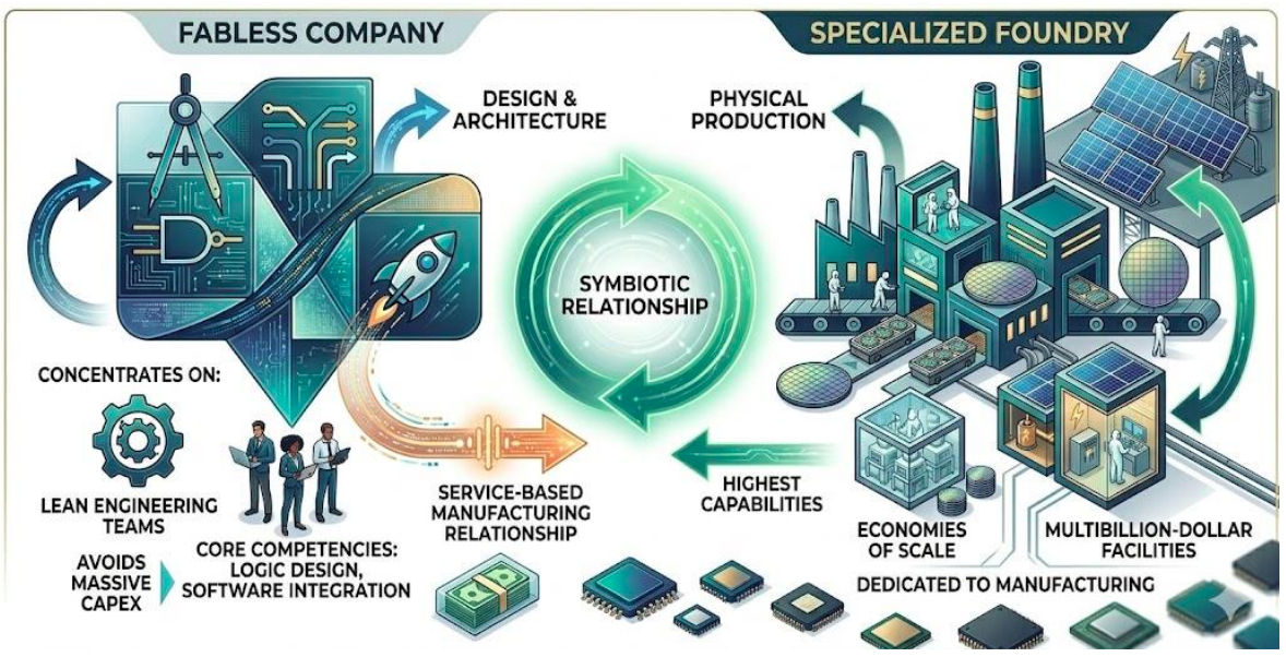
Historically, the domain of custom IC design was an exclusive preserve of large technology corporations capable of shouldering colossal capital expenditures. Constructing a state-of-the-art fab for leading-edge technologies now requires investments upwards of US$15–20B — encompassing multi-story cleanroom environments, intricate global supply chains for specialised materials, and the acquisition of ultra-expensive lithography machines such as those used for Extreme Ultraviolet (EUV) processing. This immense upfront capital requirement created a formidable moat, preventing all but the well-funded entities from participating in the creation of integrated circuits.
The economics did not merely disadvantage small companies — they made custom silicon structurally impossible for them. A startup could not amortise a $20B fab across its first product run. The minimum viable scale was tens of millions of units. For decades, this confined innovation at the silicon level to a narrow band of incumbents.
1.2 — EDA Tools: From Commercial Monopoly to Open Source
For decades, EDA software was the exclusive domain of three large, publicly-traded corporations: Synopsys, Cadence Design Systems, and Siemens EDA (formerly Mentor Graphics). Their proprietary suites, often costing hundreds of thousands of dollars per engineer per year, formed a significant part of the economic barrier that prevented smaller companies and academic institutions from entering the field of custom silicon design.
A quiet revolution has been underway since around 2016, culminating in a robust, fully-integrated, open-source EDA ecosystem capable of supporting a complete RTL-to-GDSII design flow for production-grade chips. This development has been the critical enabler for growth of the fabless model among small teams, removing the prohibitive software licensing costs that once formed the second wall after fabrication capital.
RTL (Register Transfer Level) is a hardware design abstraction describing a chip's behaviour in Verilog or VHDL — the human-readable blueprint of a digital circuit. GDSII (Graphic Data System II) is the final geometric layout file containing every transistor, wire, metal layer, and mask shape required for fabrication. The RTL-to-GDSII flow transforms an abstract functional description into a manufacturing-ready layout through synthesis, placement, routing, timing checks, and physical verification.
1.3 — The Fabless Business Model
A fabless company strategically outsources the entire physical production of its chips to specialised, independent foundries — allowing it to concentrate its resources and expertise on architecture, logic design, and software integration. The foundry achieves economies of scale by dedicating its multibillion-dollar facilities exclusively to manufacturing, serving a diverse clientele ranging from established giants to agile startups. TSMC, for example, accounted for 34% of the pure-play foundry industry in 2024.
The emergence of robust, open-source EDA toolchains has now eliminated the second major barrier to entry — the prohibitive cost of proprietary software licences. This convergence of the fabless business model and accessible design tools has created a fertile ground for innovation, empowering startups to compete in niche markets that were previously inaccessible.
1.4 — From FPGA to ASIC: A Natural Evolution
For most computer engineering professionals experienced in Xilinx FPGA-based development, the transition to ASIC design represents a natural and logical evolution. The skills acquired in defining system constraints, writing RTL in Verilog, and performing functional verification are directly transferable to the world of Application-Specific Integrated Circuit (ASIC) design.
On an FPGA, routing tracks, clock trees, and IO blocks are pre-fabricated — the Vivado tool simply routes signals through existing hardware switches. In an ASIC, every single wire, buffer, transistor, and clock distribution network must be synthesised, placed, and routed entirely from scratch onto a blank die. What Xilinx handled silently in the back-end becomes your explicit responsibility — and the open-source tools now make that responsibility tractable.
1.5 — How Large Fabs Support the Fabless Model
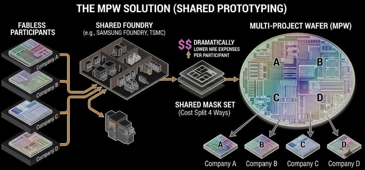
Large fabs like TSMC and Samsung Foundry solve the NRE cost problem by aggregating multiple fabless designs onto a single Multi-Project Wafer (MPW). Instead of each customer paying for an entire mask set, the MPW service partitions the reticle area, allowing up to 40–60 different designs to share the same physical masks. This substantially reduces the cost for startups.
TSMC's Open Innovation Platform® (OIP) is a cornerstone of this strategy, providing customers with Process Design Kits (PDKs) and extensive technical support to streamline the design-to-manufacturing handoff and optimise yields. SMIC, China's largest contract chip maker, leverages heavily subsidised domestic capacity expansions to aggressively price mature nodes, making it a highly competitive option for startups focused on strict unit-cost optimisation.
2 — Technology Tour: Choosing Your Node
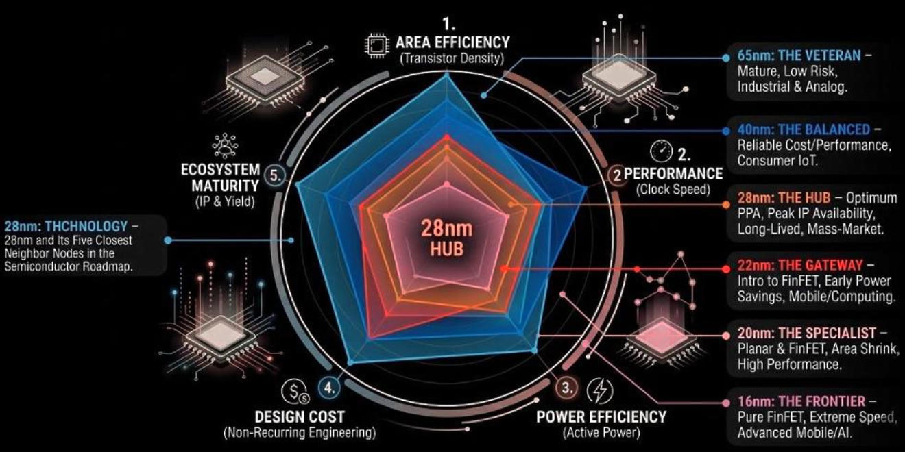
The selection of a semiconductor manufacturing technology node is arguably the most consequential commercial decision a fabless company makes. This choice dictates the chip's performance potential, power consumption, transistor density, and, most critically, its cost of production.
2.1 — The 28nm Sweet Spot
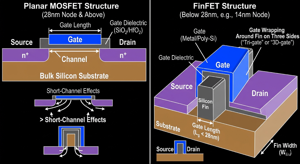
The fundamental reason for 28nm's enduring appeal lies in the stark economic divide between mature planar CMOS technology and the more advanced 3D FinFET geometries used in nodes smaller than 28nm. The 28nm process uses a planar transistor architecture — a highly evolved and perfected version of classical CMOS technology — where the gate sits flat on top of the channel.
Below 28nm, planar structures suffer from severe short-channel effects, primarily leakage current, where electrons tunnel through the increasingly thin gate oxide. To combat this, foundries adopted the FinFET (Fin Field-Effect Transistor) structure, where the gate wraps around the channel on three sides. While technologically superior, FinFETs are vastly more complex and expensive to manufacture — requiring up to 80–100 separate photomasks and, at advanced nodes, prohibitively expensive EUV lithography equipment.
Because the capital cost of 28nm equipment has already been paid off at TSMC and other foundries, they can offer 28nm manufacturing at a significantly lower price point — recovering only operational costs and profit margin, not amortising billions in new capital expenditure. This economic advantage makes 28nm exceptionally cost-effective for volume production.
2.2 — Clock Frequency and Power Envelope
The 28nm planar process is perfectly aligned with the needs of embedded processors and low-power, high-efficiency applications. Running a 28nm planar chip beyond approximately 1.5–1.8 GHz leads to a dramatic increase in power consumption and heat generation due to leakage currents and dynamic power dissipation — creating a thermal wall that is difficult and inefficient to overcome.
For a target RISC-V embedded processor running at 150 MHz, this limitation is entirely irrelevant. Even for high-performance automotive Electronic Control Units (ECUs) targeting up to 1.2 GHz, the 28nm planar process offers ample performance. For applications requiring clock speeds above 2.5 GHz — top-tier CPUs or AI training accelerators — the performance benefits of FinFET nodes may justify their premium cost. For the majority of IoT controllers, edge devices, and embedded systems, the leap to a FinFET process is economically unjustifiable.
Do not design a 28nm chip expecting to push it past 1.8 GHz in production. Leakage current and dynamic power scale super-linearly above this point on planar CMOS. Clock frequency above the thermal wall should be treated as a process selection trigger, not a design parameter — if you genuinely need 2.5 GHz+, budget for 16nm FinFET and multiply your NRE accordingly.
3 — PDKs, Tool Access, and the Hybrid Workflow
3.1 — Process Design Kits
The viability of any ASIC toolchain rests upon the Process Design Kit (PDK) — a collection of technology files provided by a semiconductor foundry containing the foundational data required to design manufacturable circuits for a specific process node. This includes transistor models, geometric design rules, parasitic extraction data, and pre-characterised standard cell libraries.
Historically, PDKs were treated as highly confidential intellectual property, accessible only under strict Non-Disclosure Agreements (NDAs). The open-source hardware movement gained critical momentum when foundries began releasing open PDKs for mature process nodes:
- SkyWater SKY130 (130nm) — Released as a fully open-source PDK, serving as the foundational proving ground for modern open-source EDA tools. The first tape-out-ready open PDK, produced in partnership with Google.
- GlobalFoundries GF180MCU (180nm) — Made publicly available, targeting low-cost, mixed-signal, and microcontroller-focused designs.
- OpenRPDK28 (28nm template) — Developed by RIOS Lab as an open-source PDK template that mimics industrial 28nm technology, enabling design exploration and layout dry-runs before porting to the secure NDA environment.
For commercial foundries such as TSMC or SMIC, access to the actual 28nm PDK requires a corporate NDA signed through a silicon broker or aggregator — MOSIS, imec IC-link, VLSIShuttle, Muse Semiconductor, or Europractice. These brokers act as the legal interface between the startup and the foundry, handling contract administration, NDA management, MPW slot booking, and sign-off verification services.
3.2 — The Hybrid Workflow for TSMC 28nm
Using open-source EDA tools to design a commercial chip on a proprietary node like TSMC 28nm is possible, but it requires a carefully managed hybrid workflow. Open-source tools like OpenROAD and Yosys are highly capable of handling the placement and routing mathematics for a 28nm design — even down to 5nm — however, TSMC will not accept a raw design file unless it has been verified by industry-standard commercial sign-off tools. The critical bridge is the silicon broker's Calibre verification service.
Legal Foundation
TSMC and silicon brokers will not sign contracts with individuals or loose collectives. Register as a formal private limited company with a commercial business address (an incubation centre works perfectly), a corporate website, and a corporate email domain. This is a non-negotiable prerequisite — not a formality.
Legal PDK Access via Broker
Apply for access through a commercial aggregator such as MOSIS, imec IC-link, or VLSIShuttle. You sign a corporate NDA with the broker — this grants your startup legal access to the TSMC 28nm PDK and standard cell libraries without requiring direct engagement with TSMC, which reserves direct customer relationships for high-volume accounts.
MOSISimec IC-linkVLSIShuttleMuse SemiExtract Non-Proprietary PDK Files
TSMC's native PDK is built for Cadence/Synopsys proprietary environments. To use open-source tools, extract the standard, non-proprietary files from inside the PDK package: .lib (Liberty timing files for synthesis), .lef (Library Exchange Format for physical cell geometries), and .v (Verilog structural models for simulation). These formats are vendor-neutral and fully compatible with Yosys and OpenROAD.
Open-Source Physical Design
Set up a containerised open-source toolchain (OpenLane or OpenROAD-flow-scripts). Use Verilator or Icarus Verilog for functional simulation. Synthesise RTL to gate-level netlist via Yosys using the extracted 28nm .lib files. Run OpenROAD for floorplanning, placement, Clock Tree Synthesis (CTS), and detailed routing using the .lef files. Output: a raw GDSII layout file ready for sign-off.
YosysOpenROADVerilatorOpenLaneKLayoutCommercial Sign-Off — The Bridge
Open-source physical verification tools (Magic, Netgen) cannot process TSMC's highly complex 28nm DRC and LVS decks. TSMC will reject any GDSII not verified by a commercial sign-off engine such as Siemens Calibre. Rather than purchasing a Calibre licence (which would cost more than the MPW slot itself), pay the silicon broker for their sign-off verification service. They run Calibre on their servers, return the error logs, and you fix the layout in your open-source tools until it passes clean.
Siemens CalibreCadence PegasusSynopsys IC ValidatorManufacturing & Packaging
Once the design passes the broker's commercial sign-off check, the broker submits the GDSII directly to TSMC for the next available MPW shuttle run. Manufactured dies arrive at your doorstep approximately 3–4 months after tape-out. Ship the bare dies to a prototype packaging service (Quik-Pak, Novapack). Packaged chips arrive 2–4 weeks after that.
TSMC CyberShuttle®SMIC MPWQuik-PakNovapack3.3 — Commercial EDA: The Startup Escape Hatch
If your startup wants to completely bypass the open-source workflow and use the official gold-standard commercial EDA software that TSMC natively accepts, EDA vendors all offer Startup Accelerator Programs that slash standard enterprise costs by 80–90%. On-premise installation requires applying to the Synopsys Startup Program or Cadence Startup Partner Program. To qualify, your company must be under 5 years old, under $10M in valuation, with annual revenue close to zero.
4 — Open-Source EDA Tooling: RTL to GDSII in Seven Steps
4.1 — FPGA vs. ASIC Architecture
In an FPGA development environment, the physical substrate is pre-fabricated — the vendor's compiler automatically maps logical operations into pre-allocated Lookup Tables, Block RAMs, and rigid global clock distribution networks. Designing an ASIC on the TSMC 28nm node requires the physical realisation of every transistor, standard cell, custom memory macro, power rail, and clock tree wire from the ground up. The transition is summarised below.
| Attribute | FPGA Prototyping | ASIC @ 28nm |
|---|---|---|
| Logic Realization | Configurable LUTs & flip-flops with fixed physical boundaries | Standard Cell Libraries — physical layouts of gates (NAND, NOR, AOI, DFF) |
| Interconnect Physics | Segmented, pre-routed copper tracks with high intrinsic resistance and programmable switch matrices | Custom-routed metal layers (9–11 copper layers) optimised for minimum wire length and delay |
| Clock Distribution | Hardwired low-skew buffers (BUFG, BUFGCE) through dedicated clock networks | Synthesised Clock Trees built from clock buffers/inverters, dynamically balanced to minimise skew and insertion delay |
| Memory Architecture | Pre-allocated BRAMs and UltraRAMs with fixed ports, aspect ratios, and positions | Custom compiler-generated SRAM macros tailored to exact word counts, bit widths, and multiplexing factors |
| Timing Sign-Off | Highly pessimistic vendor-packaged timing models; physical layout failures impossible | Multi-Corner Multi-Mode (MCMM) STA accounting for extreme physical variations and lithographic defects |
| Mistakes | Corrected with a bitstream re-upload — minutes of work | A mistake after tape-out costs months and tens of thousands of dollars to correct |
| Lithographic Constraints | Abstracted by FPGA vendor; not exposed to the engineer | Strict physical rules: double patterning, density limits, antenna effects, ESD protection |
4.2 — Environment Determinism: Docker and Nix
Before writing a single line of RTL, standardise the toolchain environment. Use Nix Flakes or Docker to package the compiler, simulator, and physical design tools with specific pinned version numbers. The Titan-I project distributes pre-built Docker containers and Nix environments containing specific, pinned versions of Verilator, Spike, and the OpenROAD toolchain — ensuring that every engineer on the team synthesises identical netlists and identical layouts. This eliminates the "works on my machine" failure mode, which is catastrophically expensive when discovered after a $60K tape-out.
4.3 — The OpenRPDK28 Bridge
Because TSMC 28nm physical design rules are protected under strict NDAs, direct integration with open-source tools can be challenging. The academic-to-industrial bridge OpenRPDK28, developed by RIOS Lab at Peking University, acts as an open-source PDK template that mimics industrial 28nm technology. It provides open-source cell libraries, symbols, and SPICE models; preliminary design rules, layer maps, and ESD structures; and runsets for physical verification (DRC/LVS). Use OpenRPDK28 for initial physical design exploration and layout dry-runs before porting the design into the secure foundry-NDA environment. This practice can catch gross physical violations before the clock is ticking on paid broker verification runs.
4.4 — Detailed Physical Design Pipeline
Step 1 — High-Level RTL Design with Chisel
Traditional Verilog and SystemVerilog are static and prone to scaling errors in highly parallel designs. For complex designs, use Chisel (Constructing Hardware in a Scala Embedded Language) — it allows hardware engineers to write object-oriented generators that programmatically output highly optimised, synthesisable Verilog, adjusting parameters such as number of execution lanes, cache size, or bus widths without error-prone manual editing. The Titan-I project uses Chisel to generate a full RISC-V vector processor from a parameterised description — changing lane count from 4 to 8 takes a parameter edit, not a Verilog rewrite.
Step 2 — Verification and Co-Simulation
Before committing to physical design, achieve full functional verification using open-source simulation engines. Verilator compiles synthesisable Verilog directly into highly optimised C++ code, achieving cycle-accurate execution speeds orders of magnitude faster than interpreted simulators like ModelSim. Cocotb drives test benches with Python co-routines, enabling modern verification techniques, assertions, and randomised testing without a commercial UVM licence.
For CPU designs, run your Verilated RTL in lockstep with the golden Spike Instruction Set Simulator. Spike checks register states on every instruction commit, flagging functional bugs instantly before synthesis. Any discrepancy between Spike's architectural model and your RTL implementation is caught at zero NRE cost — before a single dollar of mask money is spent.
Step 3 — Logic Synthesis via Yosys
Yosys, the premier open-source synthesis engine, parses SystemVerilog files, performs logical optimisations, and maps the design to the TSMC 28nm standard cells using technology mapping scripts and the extracted .lib files. Key considerations for 28nm:
- Track Height Selection: Select 7-track (7T) high-density cells for logic-heavy, area-constrained sub-blocks, or 9-track (9T) standard cells for speed-critical modules.
- Multi-Threshold Voltage (Vt) Partitioning: Map non-critical paths to high-Vt (HVT) cells to reduce static leakage current; map critical timing paths to low-Vt (LVT) cells to maximise performance.
- DFT Insertion: Insert scan chains and memory Built-In Self-Test (BIST) logic during or immediately after synthesis to make the fabricated silicon testable. Silicon testing is not optional — without DFT, a failed chip tells you nothing useful about why it failed.
Step 4 — Floorplanning and Macro Placement
Memory blocks (SRAM macros generated via TSMC's compiler) and analog IP must be floorplanned carefully. Hand-placing dozens of SRAMs in a complex vector processor often leads to routing congestion and clock distribution issues. Key rules: enforce placement halos around SRAM boundaries — keep at least 2–3 μm clear of standard cells to ensure macro pins are fully accessible by the routing engine. Design the Power Delivery Network (PDN) in OpenROAD by routing a low-impedance mesh of horizontal and vertical power straps on upper metals (M7, M8, M9) to combat dynamic IR drop, which becomes a yield risk in high-frequency designs.
Step 5 — Placement, CTS, and Routing in OpenROAD
Once the floorplan is fixed, use the OpenROAD tool suite to execute the core physical design flow autonomously:
- Global Placement (RePlAce) & Detail Placement (OpenDP): Distribute standard cells uniformly across rows. Well-tap cells must be placed every 30–40 μm to prevent latch-up.
- Clock Tree Synthesis (TritonCTS): Synthesises a balanced clock tree using symmetric H-tree topologies. Apply Non-Default Routing (NDR) rules to clock lines — double spacing and double width — to minimise clock skew and coupling jitter.
- Detailed Routing (TritonRoute): Assigns nets to specific copper tracks. At 28nm, the router must natively support double patterning (Litho-Etch-Litho-Etch, LELE) rules on lower critical metal layers (M1, M2), assigning mask colours to resolve pitch conflicts. TritonRoute must also insert antenna diodes near standard-cell inputs to prevent dielectric charge damage during plasma etching.
Step 6 — Parasitic Extraction and Static Timing Analysis
Extract actual wire resistances and capacitances to generate standard SPEF files. Run OpenSTA to verify timing across multiple corners. Unlike older nodes, 28nm requires Parametric On-Chip Variation (POCV) modelling to dynamically calculate local variations based on physical path depth — preventing overly pessimistic margins while catching real violations. Verify timing closure using standard setup and hold equations across all required PVT (Process-Voltage-Temperature) corners.
Step 7 — Physical Verification and DFM in KLayout
KLayout runs the final local verification passes before broker submission:
- DRC (Design Rule Checking): Verify minimum spacing, widths, and enclosure rules using OpenRPDK28 rule decks or the broker's preliminary decks.
- LVS (Layout vs. Schematic): Compare the extracted SPICE netlist from KLayout against the synthesised gate netlist to ensure they describe identical circuits.
- DFM (Design for Manufacturability): Run automated Python scripts in KLayout to insert dummy metal fill across empty regions — ensuring a uniform metal density profile to prevent planarisation dishing — and insert redundant vias on all critical routing paths to prevent single-via open failures in production.
4.5 — Verification Sign-Off Scenarios and Costs
The broker's sign-off verification service comes in four distinct scenarios with very different cost implications. Choosing the right scenario requires understanding your open-source toolchain's maturity and your schedule tolerance.
1–3 pre-shuttle sign-off runs are included in the baseline MPW slot price. The broker includes these to protect the rest of the wafer from being contaminated by a defective design submission.
Per run, if your open-source toolchain outputs messy GDSII that exhausts the free runs. The broker bills a flat engineering fee each time they spin up their Calibre cluster to re-verify your layout fixes.
A standalone verification run months before buying an MPW slot — to check if your open-source flow can hit 28nm metrics at all. The broker runs your GDSII through the golden deck and returns the raw Calibre error database.
The broker's physical design engineers act as your hands — actively running verification, fixing advanced 28nm issues (density violations, antenna effects, dummy metal fill), and bringing your layout to 100% compliance.
Run a Dry Run (Option C) approximately 2 months before your target MPW shuttle window. This gives you time to fix systematic flow issues — mis-configured DRC rules, layer-map errors, density violations — without burning your free shuttle-included runs on avoidable mistakes. Factor this $5–10K into your budget from day one.
5 — Titan-I: Open-Source Silicon at Scale
A common concern among system designers is whether open-source hardware tools and architectures can produce high-performance, manufacturing-worthy silicon. Historically, complex high-performance processors were considered the exclusive domain of proprietary EDA toolchains and closed-source IP. The Titan-I project challenges this view definitively.
5.1 — Project Origin
Titan-I (T1) is an open-source, high-performance out-of-order (OoO) RISC-V Vector (RVV) processor core. It was developed by a collaborative research group including Jiuyang Liu, Qinjun Li, Yunqian Luo, and Mingyu Gao, with contributions spanning Huazhong University of Science and Technology, Tsinghua University, and the Institute of Software at the Chinese Academy of Sciences (ISCAS). The processor was presented at the 58th IEEE/ACM International Symposium on Microarchitecture (MICRO 2025) in Seoul, South Korea — one of the most selective venues in computer architecture research.
5.2 — Architecture
Titan-I is designed to scale both Instruction-Level Parallelism (ILP) and Data-Level Parallelism (DLP) by decoupling scalar instruction execution from a wide, multi-lane parallel vector execution engine. The architecture fully complies with the official RISC-V Vector Extension (RVV 1.0) specification, enabling efficient parallel computation of multi-precision integers and floating-point datatypes. The microarchitecture is optimised for highly parallelised applications — deep neural networks, HPC kernels, and cryptographic workloads.
5.3 — Design and Physical Execution
Titan-I is implemented in Chisel, which raises the level of hardware design abstraction by providing object-oriented programming, functional programming, and strongly-typed parameterised generators. Instead of manual edits to static Verilog code, Chisel allows the T1 architecture to be configured programmatically — adjusting parameters such as vector register file size, vector register length, and number of physical execution lanes, causing the Chisel generator to dynamically restructure the execution datapath and output optimised synthesisable Verilog.
The physical design flow of Titan-I is executed using the open-source OpenROAD physical synthesis tool suite. This automated, scriptable flow performs physical synthesis, placement, clock tree synthesis, and detailed routing — with successful physical synthesis evaluations down to 7nm technology. This demonstrates conclusively that open-source tools can resolve the complex lithographic and electrical design rules of modern sub-10nm silicon manufacturing.
Titan-I is not an academic toy — it is a full, out-of-order vector processor synthesised to real silicon geometry using entirely free tools. The question is no longer whether open-source EDA can do this; it is whether your team is disciplined enough to execute the flow.
— On the significance of the Titan-I result6 — Foundry Economics: TSMC vs. SMIC
Once a design has been completed using an open-source toolchain and a target node selected, the next critical step is engaging with a semiconductor foundry for fabrication. The two dominant players in the mature-node space are TSMC and SMIC. While both offer 28nm manufacturing services, their business models, cost structures, and geopolitical contexts create distinctly different value propositions.
Designs containing cryptographic hardware fall under strict dual-use export regulations — the Wassenaar Arrangement and US Export Administration Regulations (EAR). Sending a tape-out with advanced crypto IP to SMIC (Mainland China) requires rigorous legal compliance, export licences, and ECCN (Export Control Classification Number) declarations. Any future regulatory changes or tightening of export controls could retroactively impact supply-chain continuity. Taping out at TSMC (Taiwan) is generally a smoother administrative process for Western entities, though ECCN declarations remain mandatory regardless of foundry choice. Retain qualified export-control legal counsel before committing to a SMIC tape-out containing crypto IP.
6.1 — MPW Silicon Fabrication Costs
Foundries and shuttle aggregators price MPW runs per square millimetre, but strictly enforce minimum area rules. Even if your chip is 3mm², you will pay for the foundry's minimum block size (often 4mm² or 9mm²). An MPW run typically delivers 40–100 bare dies.
| Foundry & Node | Est. Cost / mm² | Typical Min. Area | Estimated Silicon Cost (40–100 dies) |
|---|---|---|---|
| TSMC 28nm (HPC/HPC+) | $13K–$16K | 1mm² (mini@sic) | $52K–$64K+ (4mm²) |
| TSMC 40nm (LP/G) | $6K–$10K | 3mm² | $18K–$30K |
| SMIC 28nm (PolySiON/HKMG) | $10K–$13K | 2–5mm² | $20K–$65K |
| SMIC 40nm (LL/G) | $4K–$7K | 3–4mm² | $12K–$28K |
SMIC is generally ~30% cheaper than TSMC for mature nodes — acting as a highly competitive option if you are price-sensitive at the prototyping stage and your design does not contain regulated IP.
7 — Complete Cost Breakdown: First 50 Packaged Prototypes
Taking a design from a 100% complete GDSII to fifty packaged prototypes is a major milestone. The baseline assumption: a dual-core RISC processor with embedded SRAM, cryptographic accelerators (AES, SHA, RSA/ECC), and a Root of Trust — a realistic starting point for many security-focused embedded designs. At 40nm or 28nm with an optimised layout, this scope typically requires a die area between 4mm² and 9mm².
| Line Item | Typical Cost (TSMC 28nm) | Notes |
|---|---|---|
| MPW prototype slot (4mm², ~40–50 dies) | $52K–$64K | SMIC ~30% lower; minimum block size 4mm² even if design is smaller |
| Broker sign-off verification (Calibre) | $0–$35K | 1–3 free pre-shuttle runs included; extras $3K–$6K per run; full package $15K–$35K |
| Commercial EDA (cloud, startup pricing) | $20K–$35K | Cloud pay-per-use during final 2-month sprint; startup programmes slash enterprise rates by 80–90% |
| Prototype packaging (~50 units) | $4.5K–$8K | Open-cavity QFNs or ceramic PGAs; $2–3K setup + $50–100/chip for wire-bond assembly |
| Total | $76K–$142K | Budget $100–200K with contingency. SMIC brings this to ~$55–100K. |
7.1 — Prototype Packaging Details
Because you only need 40–50 units, designing a custom organic substrate (like a standard mass-market BGA) is entirely cost-prohibitive — custom tooling NREs alone run $10,000–$30,000 just for the substrate design. Instead, use prototype packaging services with standard, off-the-shelf packages that require no custom tooling:
- Open-Cavity QFNs or Ceramic PGAs: The die is glued into a pre-made package and wire-bonded based on a custom bonding diagram.
- Setup Fee: ~$2,000–$3,000 for creating the wire-bond profile and machine setup.
- Per-Unit Cost: ~$50–$100 per chip for low-volume manual/semi-automated assembly.
- Total: $4,500–$8,000 for approximately 50 packaged units.
7.2 — Hidden Execution Factors
Lead Times: GDSII to bare die on a mature node MPW typically takes 3–4 months. Prototype packaging adds another 2–4 weeks. You will be bound to the foundry's pre-published shuttle schedule — typically 3–4 runs per year for these specific nodes. Missing the tape-out window by even one day means waiting 3 months for the next one. Build the shuttle calendar into your project plan from day one, working backwards from your tape-out date to set RTL freeze, verification completion, and sign-off milestones.
Shuttle Access Fees: If you are not a direct customer of the foundry — which requires massive volume commitments — you will go through a Channel Partner/Aggregator. They may charge a one-time onboarding or IP-handling fee in addition to the per-slot price. Budget $2,000–$5,000 for this.
EDA Programme Timing: Synopsys and Cadence startup programme applications can take 4–8 weeks to process. Apply well before you need access — do not start this process when you are 3 weeks from your synthesis sprint.
8 — Roadmap: From First Tape-Out to Full Production
Armed with an understanding of the economic landscape, the power of open-source tools, and the technical nuances of the ASIC design flow, a clear strategic roadmap emerges. The recommended strategy is a phased approach that leverages cost-sharing manufacturing models before committing to a full production run — retiring technical risk before serious capital is spent.
Phase 1 — MPW Shuttle Prototype
Fabricate a prototype using a Multi-Project Wafer service — TSMC CyberShuttle® or SMIC MPW. The primary goal is not a final product but to validate the RTL design at the silicon level, verify real-world functionality, and collect initial yield data. This yield data provides a realistic basis for calculating per-die cost for future production runs and identifies any unforeseen physical design issues. Budget: $52K–$80K total.
Phase 2 — MLM Refinement
Based on MPW learnings, employ a Multi-Layer Mask (MLM) or Multi-Layer Reticle (MLR) service — combining up to four design layers onto a single physical mask plate. This significantly lowers the initial investment compared to a full mask set, enabling low-to-medium volume production of hundreds of units on a stable, validated design without the high cost of full-volume tooling. Budget: $200K–$600K.
Phase 3 — Full Production Run
Once the design achieves functional sign-off through an MPW shuttle, commit to a full production run: a dedicated mask set (NRE) and minimum wafer start order. Technical risk is mitigated because the design has been validated in silicon and timing closed across all required PVT corners. The financial stakes are high — but the engineering is de-risked. Budget: $1.5M+ NRE at TSMC 28nm.
The phased strategy — proving the design on an MPW shuttle, refining through a multi-layer mask run, and only then committing to a full production mask set — allows you to retire technical risk before you spend serious capital.
— The core financial discipline of fabless silicon9 — Extended Use Cases: Beyond the RISC-V Processor
The principles and workflows outlined in this guide are not limited to RISC-V embedded processors. They can be generalised to address a wide spectrum of modern computing challenges. The 28nm open-source flow is particularly well-suited to four application domains where custom silicon delivers asymmetric competitive advantage.
AI Edge Accelerators
The 28nm node is the industry's optimal sweet spot for cost-versus-performance in edge AI inference. While advanced FinFET nodes offer superior absolute power efficiency, their mask costs are prohibitive for startups and niche architectures. A 28nm HKMG process allows designers to maximise logic density within a viable economic framework. Projects like e-GPU — an open-source, configurable RISC-V platform for TinyAI devices — demonstrate the feasibility of sophisticated compute accelerators on this flow without incurring compounding software licensing costs.
Automotive ECUs
The automotive industry is moving toward mixed-criticality SoCs where multiple operational domains run concurrently on a single chip — a challenge suited to the architectural flexibility of RISC-V. While safety-critical drive systems require ISO 26262 toolchain qualifications that open-source tools are still maturing toward, the open-flow is highly disruptive for secure telematics, infotainment, and V2X communication research. The Titan-I project's chiplet-based RISC-V SoC for secure nano-UAVs demonstrates the potential for heterogeneous, highly secure architectures using this decentralised methodology.
Edge Computing & IoT
The 28nm process excels in this domain by providing frequency scaling for real-time sensor fusion and local data processing while maintaining a compact physical footprint. By utilising an open-source flow, designers can strip away generic, redundant IP blocks found in commercial microcontrollers — engineering a lean, workload-optimised SoC that minimises active power dissipation. The UET-RVMCU project demonstrated successful transformation of an application-class SoC architecture into a streamlined, feature-rich microcontroller using this open-source physical design flow.
Cryptographic Hardware
The open-source nature of the entire toolchain — from processor core to physical design synthesis — enables unprecedented transparency for security auditing and custom cryptographic extensions. Hardware-native AES, SHA-3, RSA/ECC, and post-quantum lattice cores can be implemented with full auditability at the RTL and GDSII level — a feature impossible with closed commercial IP. Note: designs containing cryptographic IP are subject to strict Wassenaar/EAR dual-use export regulations regardless of foundry choice. Retain qualified export-control counsel before tape-out.
10 — Final Words
The path to fabless ASIC design has never been more open to small teams. Two barriers that once confined custom silicon to a handful of corporations — the multibillion-dollar fabrication plant and the six-figure-per-seat EDA licence — have effectively fallen away. The fabless model lets you rent world-class manufacturing through Multi-Project Wafer shuttles, while a mature open-source toolchain now carries a design all the way from RTL to a manufacturable GDSII layout. For an engineer already fluent in FPGA development, the front-end skills transfer almost directly; what you are really learning is the discipline of the back-end physical flow.
That openness is not the same as ease, and it is worth being honest about what the journey demands. Unlike an FPGA bitstream, a fabricated die cannot be re-uploaded — a mistake caught after tape-out costs months and tens of thousands of dollars to correct. Foundries still require final sign-off on certified commercial tools, so a hybrid flow and a working relationship with a silicon broker are unavoidable. Foundry selection is a genuine trade-off: TSMC offers premium yield and a rich IP ecosystem at a higher price, while SMIC is markedly cheaper but carries geopolitical and export-control exposure that must be managed deliberately — particularly for designs containing cryptographic IP. None of these obstacles is disqualifying, but each rewards planning over improvisation.
Taken as a whole, it is the economics that make the opportunity compelling. A complete, state-of-the-art design environment is now within reach of a modest budget, and the phased strategy recommended in this paper — proving the design on an MPW shuttle, refining it through a multi-layer mask run, and only then committing to a full production mask set — allows you to retire technical risk before you spend serious capital. The 28nm planar node sits at the centre of this strategy, offering the rare convergence of low cost, ample performance, and proven manufacturability for the embedded controllers, AI accelerators, automotive subsystems, and edge devices where most startups will compete.
For founders willing to pair that engineering discipline with sound commercial judgment, the reward is substantial: the ability to build differentiated, workload-optimised silicon that was, until very recently, the exclusive territory of the largest semiconductor firms.
The tools, the foundry access, and the business model are all in place. What remains is the decision to begin — and the teams that move thoughtfully now will be the ones that define the next generation of custom hardware.
[1] TSMC Open Innovation Platform® (OIP) — tsmc.com/english/dedicatedFoundry/services/Open_Innovation_Platform
[2] SkyWater SKY130 Open PDK — github.com/google/skywater-pdk
[3] GlobalFoundries GF180MCU Open PDK — github.com/google/gf180mcu-pdk
[4] OpenROAD Project — openroad.readthedocs.io
[5] Yosys Open Synthesis Suite — yosyshq.net/yosys
[6] KLayout — klayout.de
[7] Verilator — veripool.org/verilator
[8] OpenRPDK28, RIOS Lab — github.com/rioslab/openrpdk28
[9] Liu, J. et al.: Titan-I, IEEE/ACM MICRO 2025, Seoul (2025)
[10] Chisel Hardware Construction Language — chisel-lang.org
[11] Spike RISC-V ISA Simulator — github.com/riscv-software-src/riscv-isa-sim
[12] OpenLane ASIC Flow — github.com/The-OpenROAD-Project/OpenLane
[13] Siemens Calibre — eda.sw.siemens.com/en-US/ic/calibre
[14] MOSIS Service — mosis.com
[15] imec IC-link MPW — iclink.imec.be
[16] Synopsys Startup Program — synopsys.com/company/programs/startup-program
[17] Cadence Startup Partner Program — cadence.com
[18] Wassenaar Arrangement — wassenaar.org
[19] US Export Administration Regulations (EAR) — bis.doc.gov
[20] RISC-V International Vector Extension (RVV 1.0) — riscv.org/specifications
[21] Cocotb — docs.cocotb.org
[22] e-GPU TinyAI Platform — github.com/e-GPU
[23] UET-RVMCU Project — github.com/uet-rvmcu
[24] Europractice MPW Service — europractice-ic.com
[25] Muse Semiconductor — musesemi.com